


Please Leave Us A Message
Privacy statement: Your privacy is very important to Us. Our company promises not to disclose your personal information to any external company with out your explicit permission.

 August 23, 2023


Package defects in the lead-type LED CHIP packaging process are inevitable. Based on the photovoltaic effect and electron tunneling effect of pn junction, the influence of a package defect on the photocurrent of the LED support loop was analyzed. The non-contact detection of the LED bracket circuit photocurrent is carried out by the law of electromagnetic induction, and the functional status of the LED chip and the electrical connection between the chip electrode and the lead frame are obtained, and the influencing factors of the detection accuracy are analyzed. Experiments show that the method has high detection signal-to-noise ratio and can detect the functional status and package defects of the LED chip in the packaging process. The calculation results are in good agreement with the experimental results.
Key words: LED chip; package defect detection; pn junction photovoltaic effect; electron tunneling effect; non-metal film layer
LED (Light-emitting diode) is widely used in the fields of indication, display, etc. due to its long life and low energy consumption. Reliability, stability, and high light output are factors that must be considered when LEDs replace existing lighting sources. The packaging process is one of the main factors affecting the function of the LED. The key processes of the packaging process include mounting, pressure welding and packaging. Due to the packaging process itself, there are many defects in the LED packaging process (such as repeated soldering, chip electrode oxidation, etc.), statistical data shows [1-2]: the failure rate of the soldering system accounts for 25% of the total semiconductor failure mode~ 30%, in China [3], due to the double restrictions on equipment and production, most manufacturers use manual welding methods, welding systems fail to account for more than 40% of the total number of unqualified. From the point of view of use, the defects generated in the LED packaging process, although the initial use does not affect its photoelectric performance, will gradually be exposed in the future use and cause device failure. In some applications of LEDs, such as high-precision aerospace equipment, the potential drawbacks are more harmful than those that are immediately fatal. Therefore, how to realize the detection of the LED chip in the packaging process, and block the defective LED into the subsequent packaging process, thereby reducing the production cost, improving the quality of the product, and avoiding the use of defective LEDs to cause significant loss, thereby becoming the LED packaging industry. The problem that needs to be solved urgently.
At present, the detection technology of the LED industry mainly focuses on the inspection of wafer level before packaging [4-5] and the finished product inspection after packaging [6-7], while the domestic detection technology for LED in the packaging process is still not mature. Based on the non-contact detection method of LED chip [8-9], in the LED lead package process, the pn junction photovoltaic effect is used to analyze the loop light generated by the package defect on the light-emitting LED chip in the lead frame. The influence of current is measured by the law of electromagnetic induction to realize the detection of chip quality and package defects in the LED packaging process.
1 theoretical analysis
1.1 Photovoltaic effect of pn junction [m] According to the pn junction photovoltaic effect, the photogenerated current IL is expressed as:
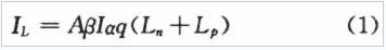
Where A is the pn junction area, q is the electron charge, Ln and Lp are the diffusion lengths of electrons and holes, J is the average light intensity calculated as the number of photons, α is the absorption coefficient of the pn junction material, and β is the quantum The yield, that is, the number of electron-hole pairs generated per absorption of one photon.
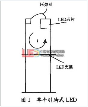
In the LED lead package process, each LED chip is fixed on the lead frame, and the LED chip forms a closed loop with the lead frame by pressure welding gold wire (aluminum wire), as shown in FIG. If the lead frame resistance is ignored, the LED holder loop photocurrent is equal to the chip photo-generated current IL. It can be seen that when the pn junction material and the doping concentration are constant, the photocurrent of the support loop is proportional to the illumination intensity I.
1.2 package defect mechanism
When the LED chip is affected by corrosion factors or contaminated with oil, a non-metal film is formed on the surface of the chip electrode to cause package defects [11]. After the electrode chip bonding process of the non-metal film layer on the surface of the electrode, a metal-medium-metal structure, also referred to as a tunnel junction, is formed at the solder joint. When a certain intensity of light is irradiated on the LED chip, if the LED chip fails, no light current flows through the support loop. If the non-metal film layer is thick enough, only a very small number of electrons can tunnel through the barrier barrier, and the LED support loop also has no photocurrent flow. If the non-metal film layer is thin, since the photo-generated current of the LED chip forms an electric field on both sides of the tunnel junction, electrons mainly tunnel through the film layer in a field emission manner, and the current flowing through the unit-area film layer can be expressed as [12].

Where q is the electron charge, m is the electron mass, 矗 is the Planck constant, vx, vy, vz are the tunneling speeds of electrons in the x, y, and z directions, respectively, and T(x) is the tunneling probability of electrons. The electron tunneling probability of any barrier can be expressed as [13]

Among them jin, jout. The current density entering the film layer and passing through the film layer, respectively.

x points to the surface of the chip electrode to the pad, which is the barrier at any point in the z-direction of the film layer, and E is the energy of the surface velocity of the vertical chip electrode as vx electrons.

2 is a barrier diagram of the surface of the 'F chip electrode at the electric field f', where EF is the Fermi level and U' is the electron emission barrier. Figure
2. If the surface of the chip electrode is abrupt, its value is U0, the electric field intensity formed by the photo-generated current on both sides of the tunnel junction is F, and the barrier outside the surface of the electrode is U0-qFx. Take the bottom of the chip electrode as the reference level E0 (x=0), so there is x<0, U(x)=0; x>0, U(x)=U0-qFx, according to the condition U(x) )=E=U0- qFx2

Where d is the thickness of the film layer and V is the voltage across the junction of the film layer. When the photo-voltaic effect occurs in the LED chip, it can be known from the formula (7) that the current flowing through the non-metal film layer on the surface of the chip electrode is affected by the thickness of the film layer, and as the film layer is thickened, the current flowing through the film layer is reduced. The photocurrent flowing through the LED holder loop will also decrease.
In summary, the presence or absence of the photocurrent of the lead LED bracket can reflect the functional status of the LED chip in the packaging process and the electrical connection between the chip electrode and the lead frame. Therefore, it can be detected by detecting the photocurrent of the LED support loop. Detect chip functional status and package defects in the lead package process.
1.3 Detection method of package defects
After the completion of the pressure welding process, the LED is in a closed short circuit state, and it is not feasible to directly derive the loop current for detection. Although the support loop has a certain resistance, the photo-generated current is only on the order of micro-ampere, so the voltage drop in the support loop is very small, and the general voltage measurement method is difficult, and the contact detection will introduce contact resistance, which affects the accuracy of the detection. . Therefore, a non-contact current detecting method is considered. According to Faraday's law of electromagnetic induction, using the characteristics of the lead-type LED, the end of the magnetic core with the magnetic core coil is inserted into the closed circuit z shown in Fig. 1, and the LED support circuit is used as the primary winding with the magnetic core coil as the secondary The winding is connected, and the capacitor C is connected in parallel at both ends of the coil, and the coil L constitutes an LC resonant circuit. When the LED chip is excited by the alternating light, an alternating current is generated in the bracket circuit, the alternating current carrying circuit generates an alternating magnetic field in the surrounding space, and the alternating magnetic field of the secondary coil generates an induced electromotive force in the secondary coil. If the alternating optical frequency is equal to the LC resonant tank frequency, the LC loop resonates, and the induced electromotive force is maximized at both ends of the secondary coil. Therefore, the purpose of detecting the photocurrent of the support loop can be indirectly achieved by detecting the induced electromotive force at both ends of the secondary coil, thereby realizing the detection of the function state of the chip and the quality of the solder in the packaging process.
In the LC resonant circuit, the magnetic core in the coil acts to enhance the magnetic induction B, thereby increasing the amplitude of the detection signal. The relationship between the effective permeability and the relative permeability of the core in the coil can be expressed as [14]:

Where, the effective magnetic permeability of the μe core is the relative magnetic permeability of the magnetic core, and μr is the effective magnetic path length of the magnetic core, which is called the non-closed air gap length.
It can be seen from equation (8) that the parameters affecting the effective magnetic permeability threat and affecting the magnetic induction B are:
1 relative magnetic permeability of the core material. It is related to the selected soft magnetic core material (the initial relative magnetic permeability of the soft magnetic material is generally greater than 1000), and the relative magnetic permeability is determined when the core material is selected.
2 The effective length of the magnetic core, the length of the non-closed air gap lg, which are determined by the structure of the magnetic core. The magnetic field generated by the weak current is easily interfered by external factors. The longer the magnetic circuit, the greater the interference, so the effective length of the core should be short.
In the case where the core material is determined, in order to obtain a large magnetic induction B, it is necessary to change the structure of the core in the coil. If the core structure is designed to be ring-shaped, it is known from equation (8) that the magnetic induction B is increased by a factor that is theoretically equal to the relative magnetic permeability of the core, and the amplitude of the detection signal will be maximized. A strip core is formed on the u-shaped core of the same material as the strip core to form a toroidal core coil, and there are two ways of overlapping, as shown in FIG.

During the detection, one end of the U-shaped core around the coil is inserted into the 1 closed loop shown in FIG. 1 to sense the alternating magnetic flux generated by the loop current in the LED bracket loop, and then the strip core is overlapped on the U-shaped core. , the induction magnetic circuit is closed. Due to the different lap joints, the magnetic coils of the two lap joints are in the alternating magnetic field generated by the bracket circuit, and the magnetic circuit at the lap joints will be different. The magnetics of the two lap joints are simulated by Ansoft Maxwell software. The core overlaps the magnetic circuit in the alternating magnetic field, and the result is shown in FIG.

The simulation results of (a) and (b) in Fig. 4 correspond to the two coil core bonding methods in (a) and (b) of Fig. 3. Comparing the simulation results of the magnetic circuit at the junction of the two coil cores, it can be seen that: 1Fig. 3(a) shows that the magnetic circuit in the core overlap has the shortest circuit in the air medium, and the magnetic reluctance is the smallest, so the magnetic loss is also the smallest. . 2Because the loop current of the LED bracket to be tested is in the order of micro-ampere, the excited magnetic field is small and is easily interfered by the space electromagnetic field. Figure 3(b) shows that the magnetic circuit at the core overlap is exposed to more air medium. The probability of interference is large. According to the above analysis, FIG. 3(a) has better magnetic core bonding mode, which can enhance the signal detection end to suppress the interference capability, increase the detection signal amplitude, and improve the signal-to-noise ratio of the optical excitation detection signal to a certain extent, thereby improving the defect detection precision.
2 experiment and analysis
2.1 experiment
In order to compare the influence of the strip core coil and the toroidal core coil on the detection accuracy of the package defect, experiments were carried out using a strip core coil and a toroidal core coil as shown in Fig. 3(a), respectively. The magnetic core material is PC40, its initial relative magnetic permeability is about 2300, the strip core has an outer geometrical dimension of 1.6minx3.2ram×20mm, the number of turns of the coil is 300匝, and the cross-sectional dimension of the toroidal core is 1.6mm×3.2. Mm, the effective magnetic path length is approximately equal to the strip core, and the number of turns of the coil is 300 匝. In the experiment, the excitation light source is an ultra-high brightness patch type white LED. The excitation light source is driven by a square wave signal with a duty ratio of 50%. The square wave signal can be superimposed by a series of sinusoidal signals to make its fundamental frequency and The working frequency of the resonant circuit is the same, that is, the LC resonant circuit realizes the frequency selection of the square wave signal, so the rate of change of the flux linkage through the coil is the rate of change of the square wave fundamental frequency signal; the detection object is GaP material 12 mil yellow welding quality Qualified LEDs and chip electrodes in the soldering process have non-metallic film LEDs. The signal output from both ends of the coil is amplified, filtered, and peak-detected as shown in Figure 5. The amplification factor of the amplifier in the experiment was 103 times.


2.2 Analysis of results
The LED chip package defect detection method described in this paper is indirectly realized by detecting the photocurrent of the LED support loop. It can be seen from Fig. 5 that the magnetic field excited by the photocurrent of the support loop has different electromotive force at different ends of the coil of different core structure; the difference of the signal-to-noise ratio of the detection signal is different for different core structure coils. The specific performance is:
1 The welding quality qualified LED, the experimental detection value is consistent with the theoretical calculation value. Fig. 5(a) shows the experimental results of using a strip-shaped coil core. In the packaging process, the LED with acceptable soldering quality is amplified, filtered, and peak-detected with an amplitude of about 60 mV. The 12 mil yellow LED chip was selected for theoretical calculation. The chip area A=0.3 mm×0.3 mm, taking β=0.5, the average light intensity (in photons) per unit area absorbed by the semiconductor material per unit time is 5.45×10 21 / At m2s, the photo-generated current can be calculated from equation (1) to be approximately 42 μA. According to Biot-Savar's theorem, superposition theorem and Faraday's law of electromagnetic induction, the amplitude of the electromotive force induced by the 12mil yellow LED chip at the signal detection end is about 63mV, and the experimental error and calculation error are removed. The theoretical and experimental values are compared. Good match.
2 For the annular structure core coil, the experimental value is smaller than the theoretical value. According to the formula (8), for the strip-shaped magnetic core coil, it is assumed that the magnetic core effective magnetic path length le = 100 lg, and the effective magnetic permeability μe ≈ 100 at this time. If the magnetic core is changed to a ring shape, the non-closed air gap length lg ≈ 0, and the effective magnetic permeability μe ≈ μr = 2300 at this time, it can be known from theoretical calculation that the 12 mil yellow welding quality qualified LED induces an electromotive force amplitude at the signal detecting end. It is 1.4V; as shown in Fig. 5(b), the experimental result is about 220mV, and the experimental value is much smaller than the theoretical value. The above calculation is carried out under ideal conditions. In the actual experiment, the toroidal core coil is made up of a U-shaped magnetic core and a strip-shaped magnetic core, and the air gap lg at the junction still exists, so the magnetic circuit is not It may be completely closed. It is known from equation (8) that the air gap has a great influence on the effective magnetic permeability, so the effective magnetic permeability is still smaller than the relative magnetic permeability, and therefore, the experimental value is much smaller than the theoretical value.
3 Different magnetic core structures can realize the detection of LED package defects, but the signal-to-noise ratio of the detection signals is quite different. It can be seen from Fig. 5 that although the magnetic core coils have different structures in the experiment, the light excitation detection signals of the LEDs with good soldering quality are significantly larger than the LED light excitation detection signals of the non-metal film on the surface of the chip electrodes during the packaging process. Comparing the magnitudes of the detection signals of the two, the LEDs with non-metal films on the surface of the chip electrodes during the packaging process can be removed. In Fig. 5(a), the core used in the experiment has a strip-shaped structure, and there is an air gap lg. The magnetic induction intensity B is a multiple of the effective permeability μe, and the detection signal is susceptible to external interference, so the amplitude of the detection signal is relatively high. Small and large detection noise, the signal-to-noise ratio of the two chip optical excitation signals is small, which brings difficulty to the back-end signal processing and affects the accuracy of package defect detection. The magnetic core of the coil is looped to form a closed magnetic circuit, and the magnetic induction intensity B is effectively enhanced, the magnetic loss is small, and the interference by the space electromagnetic field is relatively small, so the signal-to-noise ratio of the detection signal is significantly improved.
4 different core structure affects the operating frequency of the resonant tank. During the experiment, the capacitance C of the LC resonant circuit is equal, and the effective magnetic permeability of the toroidal core is greater than the effective magnetic permeability of the strip core. Therefore, the inductance L of the toroidal core coil is larger than the inductance of the strip core coil, so The resonant frequency of the resonant circuit is small; as can be seen from Fig. 5, the resonant frequency of the resonant circuit formed by the strip core coil is about 9.75 kHz, and the resonant frequency of the resonant loop formed by the toroidal core coil is about 7.33 kHz.
5 theoretical analysis and experimental results analysis, the method has high detection accuracy for the LED bracket loop current, by detecting the magnetic field excited by the bracket loop current, the electromotive force is induced at both ends of the coil, and the LED with qualified welding quality The detection signals are compared to implement detection of LEDs having package defects during the packaging process.
3 conclusions
Aiming at the problem of package defects in the process of pin-type LED chip packaging, based on the photovoltaic effect of pn junction, the effect of a package defect on LED performance was analyzed by electron tunneling effect. Theoretical analysis shows that when there is a non-metal film on the surface of the LED chip electrode, the photocurrent flowing through the LED support loop is smaller than the photo-generated current. As the thickness of the film increases, the loop photocurrent decreases and the detection signal decreases. The non-contact method is used to detect the LED light excitation signal to be tested and compared with the qualified LED light excitation signal, thereby realizing the detection of the functional state and package defects of the lead-packaged LED chip during/after the pressure welding process. Factors affecting the accuracy of the detection were analyzed. Experiments were carried out on 12 mil yellow LED samples with non-metallic film on the surface of the chip electrode. The results show that the method can detect the micro-amplifier photo-generated current signal of the LED support circuit and has a high signal-to-noise ratio. The distinction between soldering quality and chip failure or LED with package defects can achieve the purpose of detecting the functional status and package defects of the LED chip during/after the bonding process, thereby reducing LED production cost, improving product quality, and avoiding the existence of Defective LEDs cause significant losses.
The above is the Detection method of LED Chip defects research. we have listed for you. You can submit the following form to obtain more industry information we provide for you.
You can visit our website or contact us, and we will provide the latest consultation and solutions
Send Inquiry
Most Popular
lastest New
Send Inquiry
Related Products List
Contact Us

Mobile Site
Privacy statement: Your privacy is very important to Us. Our company promises not to disclose your personal information to any external company with out your explicit permission.
Fill in more information so that we can get in touch with you faster
Privacy statement: Your privacy is very important to Us. Our company promises not to disclose your personal information to any external company with out your explicit permission.